- 您现在的位置:买卖IC网 > Sheet目录484 > NP110N04PDG-E1-AY (Renesas Electronics America)MOSFET N-CH 40V MP-25ZP/TO-263
NP110N04PDG
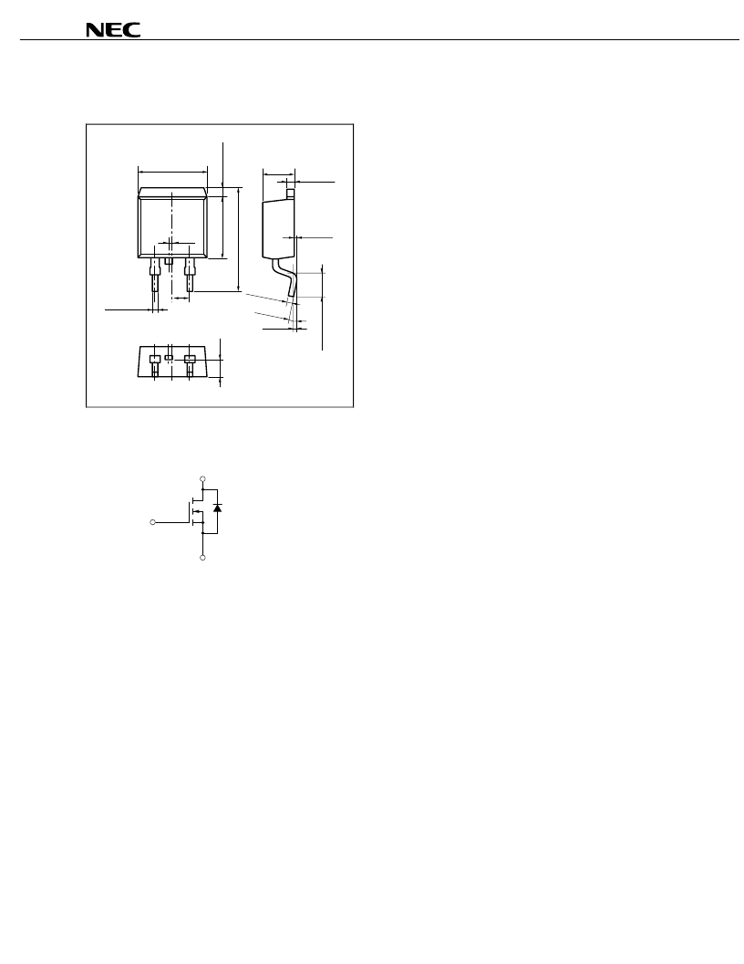
PACKAGE DRAWING (Unit: mm)
TO-263 (MP-25ZP)
10.0 ±0.3
4.45 ±0.2
1.3 ±0.2
4
0.025
0.5
to 0.25
0.6 ±0
.2
0.75 ±0.2
2.54
0 to 8
?
0.25
1 2
3
1. Gate
2. Drain
3. Source
4. Fin (Drain)
EQUIVALENT CIRCUIT
Drain
Body
Gate
Diode
Source
Remark Strong electric field, when exposed to this device, can cause destruction of the gate oxide and ultimately
degrade the device operation. Steps must be taken to stop generation of static electricity as much as
possible, and quickly dissipate it once, when it has occurred.
6
Data Sheet D17561EJ2V0DS
发布紧急采购,3分钟左右您将得到回复。
相关PDF资料
NP110N04PUG-E1-AY
MOSFET N-CH 40V MP-25ZP/TO-263
NP110N04PUJ-E1B-AY
MOSFET N-CH 40V MP-25ZP/TO-263
NP110N055PUG-E2-AY
MOSFET N-CH 55V MP-25ZP/TO-263
NP110N055PUJ-E2B-AY
MOSFET N-CH 55V MP-25ZP/TO-263
NP15P06SLG-E1-AY
MOSFET P-CH -60V MP-3ZK/TO-252
NP160N04TUG-E1-AY
MOSFET N-CH 40V 160A TO-263-7
NP161N04TUG-E1-AY
MOSFET N-CH 40V 160A TO-263-7
NP180N04TUG-E1-AY
MOSFET N-CH 40V 180A TO-263-7
相关代理商/技术参数
NP110N04PDG-E1-AZ
制造商:Renesas Electronics Corporation 功能描述:Transistor,FET,Nch,40V/110A,Tch175
NP110N04PUG(1)-E1-AY/K
制造商:Renesas Electronics Corporation 功能描述:
NP110N04PUG-E1-AY
功能描述:MOSFET N-CH 40V MP-25ZP/TO-263 RoHS:是 类别:分离式半导体产品 >> FET - 单 系列:- 标准包装:1,000 系列:MESH OVERLAY™ FET 型:MOSFET N 通道,金属氧化物 FET 特点:逻辑电平门 漏极至源极电压(Vdss):200V 电流 - 连续漏极(Id) @ 25° C:18A 开态Rds(最大)@ Id, Vgs @ 25° C:180 毫欧 @ 9A,10V Id 时的 Vgs(th)(最大):4V @ 250µA 闸电荷(Qg) @ Vgs:72nC @ 10V 输入电容 (Ciss) @ Vds:1560pF @ 25V 功率 - 最大:40W 安装类型:通孔 封装/外壳:TO-220-3 整包 供应商设备封装:TO-220FP 包装:管件
NP110N04PUG-E1-AZ
制造商:Renesas Electronics Corporation 功能描述:Transistor,FET,Nch,40V/110A,Tch175
NP110N04PUJ
制造商:RENESAS 制造商全称:Renesas Technology Corp 功能描述:MOS FIELD EFFECT TRANSISTOR
NP110N04PUJ-E1B-AY
功能描述:MOSFET N-CH 40V MP-25ZP/TO-263 RoHS:是 类别:分离式半导体产品 >> FET - 单 系列:- 标准包装:1,000 系列:MESH OVERLAY™ FET 型:MOSFET N 通道,金属氧化物 FET 特点:逻辑电平门 漏极至源极电压(Vdss):200V 电流 - 连续漏极(Id) @ 25° C:18A 开态Rds(最大)@ Id, Vgs @ 25° C:180 毫欧 @ 9A,10V Id 时的 Vgs(th)(最大):4V @ 250µA 闸电荷(Qg) @ Vgs:72nC @ 10V 输入电容 (Ciss) @ Vds:1560pF @ 25V 功率 - 最大:40W 安装类型:通孔 封装/外壳:TO-220-3 整包 供应商设备封装:TO-220FP 包装:管件
NP110N04PUJ-E2B-AY
制造商:RENESAS 制造商全称:Renesas Technology Corp 功能描述:MOS FIELD EFFECT TRANSISTOR
NP110N04PUK
制造商:RENESAS 制造商全称:Renesas Technology Corp 功能描述:MOS FIELD EFFECT TRANSISTOR
